2025/12/08
2025/11/05
2025/11/05
NOVOSENSE has launched 120V half-bridge driver NSD1224 series, which have 3A/-4A peak driver current capability, are integrated with high-voltage bootstrap diode, and are available in different versions including enabling, interlock and undervoltage protection, as well as various packages including SOP8, HSOP8, DFN10 and DFN8. It is widely used in micro inverter, power optimizer, power module, new energy vehicle and other application scenarios.
I NSD1224 features:
l Withstand voltage of VDD power of 20V
l Withstand voltage at HSpin of -10V to 115V
l Negative withstand voltage of input pin of -10V
l HS pin withstand dv/dt up to 50V/nsPeak driver current 3A/-4A
l Compatible with CMOS/TTL level input
l Input interlock function
l Independent UVLO protection for high-side and low-side output
l Integrated high voltage bootstrap diode
l Input/output delay of less than 16ns
l transmission delay matching between high and low sides is less than 1ns
l DFN10 package with enabling pin for static power consumption as low as 7uA in standby mode
l Package available in SOP8, HSOP8, DFN10 and DFN8
l Junction temperature range of -40°C to 150°C
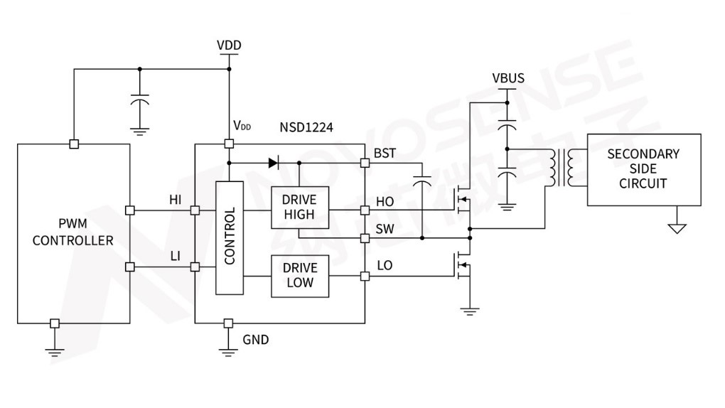
Typical application block diagram of NSD1224
II NSD1224 performance advantage:
1. NSD1224 has interlock function, which can effectively avoid shoot through of power satgedue to input interference.
In the power supply application, the input pin of the half-bridge driver chip is susceptible to interference due to the influence of high-frequency switching noise, which may cause input high at both the high and low sides, resulting in output high at both the high and low sides of the driver chip, cause shoot through of power stage , and damage to the power supply equipment.
The NSD1224 triggers an interlock mode when both inputs are high levels at the same time, in which case both the high-side and low-side output low at the same time, and only when either input becomes low level will the output return to the normal state following the input. The interlock function of NSD1224 effectively avoids shoot through caused by input signal interference, and improves the reliability of the system.
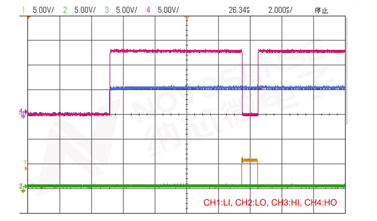
Test waveform of NSD1224 interlock function
2. The input pin of NSD1224 can withstand a negative voltage of -10V, which solves the problem of negative voltage peak in the input of the driver chip.
In power applications, due to the influence of MOSFET high frequency switches, transient current will be generated in the GND circuit, and there will be parasitic inductance due to the PCB wiring between the controller and the driver. The interaction between the transient current and the parasitic inductance will produce a negative voltage peak in the input pin of the driver chip, resulting in the logic error or even damage of the driver chip. The NSD1224 input pin is improved in respect of the negative withstand voltage, which can be of -10V (recommended working value: -5V), thereby improving the reliability of the chip and lowering the requirements for system design.
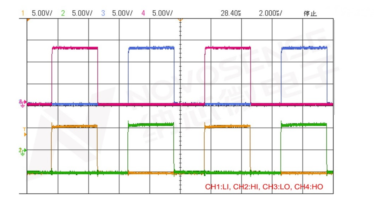
Negative withstand voltage test waveform of NSD1224 input
3. NSD1224 with HS pin with a negative withstand voltage of -10V and dv/dt immunity of 50V/ns, applicable for high-frequency and efficient switching power supply applications.
With the continuous improvement of power efficiency requirements, the switching speed of MOSFET is becoming faster and faster, so as to reduce switching losses. The di/dt and parasitic inductance caused by high-speed switching will generate transient negative voltage in the HS pin, which is likely to cause the driver chip to be locked or even damaged. The HS pin of NSD1224 can withstand negative voltage of -10V (recommended working value: -8V), which effectively solves the application problem of high-frequency and efficient switching power supply. In addition, the HS pin of the NSD1224 can withstand 50V/ns common-mode transients and has strong resistance to common-mode interference.
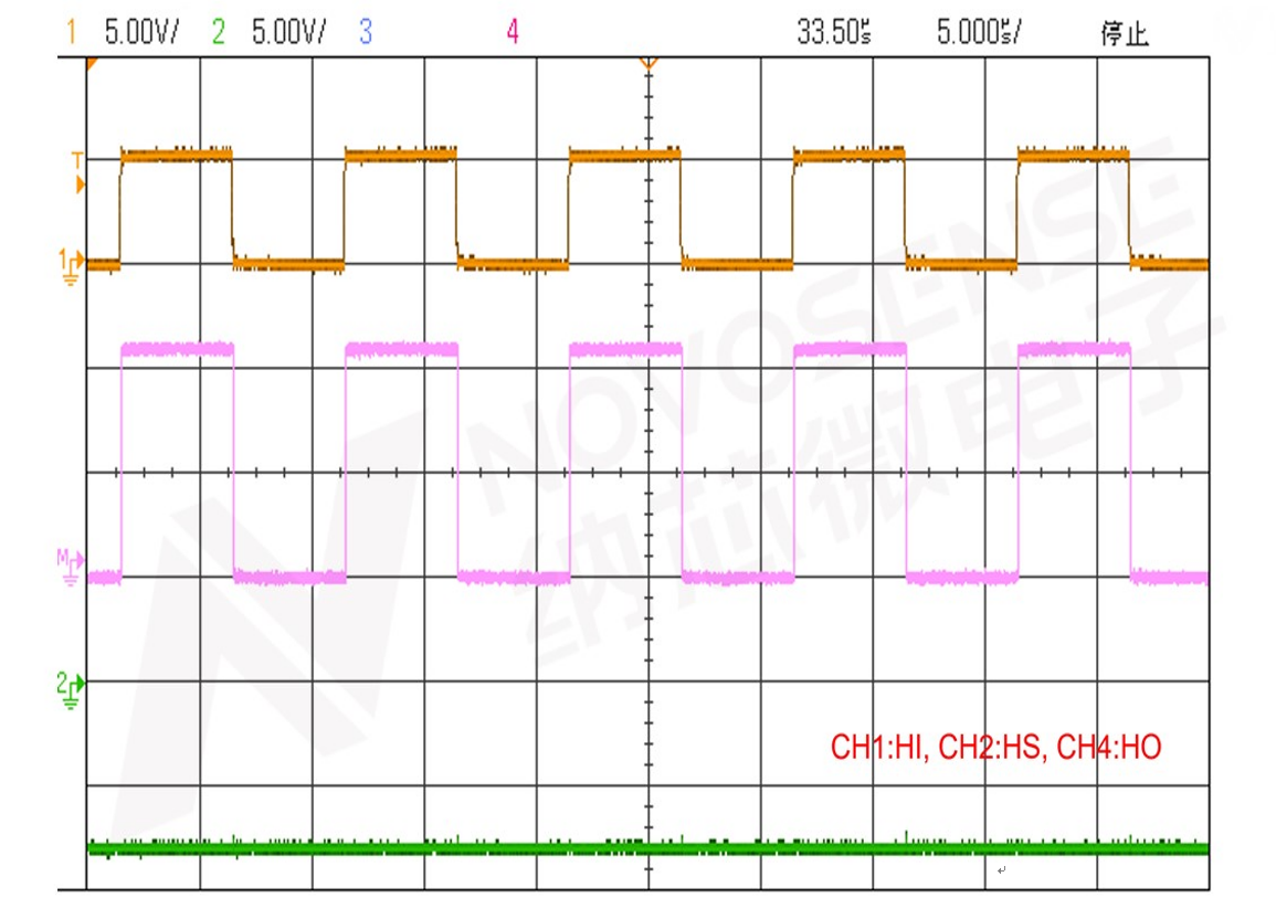
Negative withstand voltage test waveform of NSD1224 HS pin
III List of NSD1224 series
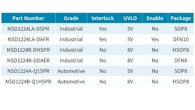
NSD1224 is available for sample. For sample application or order, please email to sales@novosns.com. For more information, click www.novosns.com.