2025/12/08
2025/11/05
2025/11/05
2025/01/06
NOVOSENSE has officially launched the NSI67x0 series of smart isolated drivers with Isolated Analog Sensing function. Suitable for driving power devices such as SiC, IGBTs and MOSFETs, and available in both automotive (AEC-Q100 compliant) and industrial variants, this series can be widely used in new energy vehicles, air conditioners, power supplies, photovoltaics and other applications.

This series of isolated gate drivers equates an isolated analog to PWM sensor, which can be used for temperature or voltage detection. The design further enhances driver versatility, simplifies system design, effectively reduces system size and lowers overall cost.
High-voltage Drive and Ultra-high Common-mode Immunity
Designed to drive IGBTs or SiC up to 2121V DC operating voltage, NSI67x0 offers advanced protection functions, excellent dynamic performance, and outstanding robustness. This series uses SiO2 capacitor isolation technology to isolate the input side from the output side, providing ultra-high common-mode immunity (CMTI>150kV/μs) while ensuring extremely small offset between devices, which is at the leading level in the industry.
Powerful Output Capability and Miniaturized Package
The NSI67x0 series has powerful output capability, supporting ±10A drive current and a maximum output drive voltage of 36V, far exceeding most similar products. Its SOW16 package design further enhances safety by achieving a creepage distance of more than 8mm while maintaining miniaturization.
Comprehensive Protection Functions and Automotive Certification
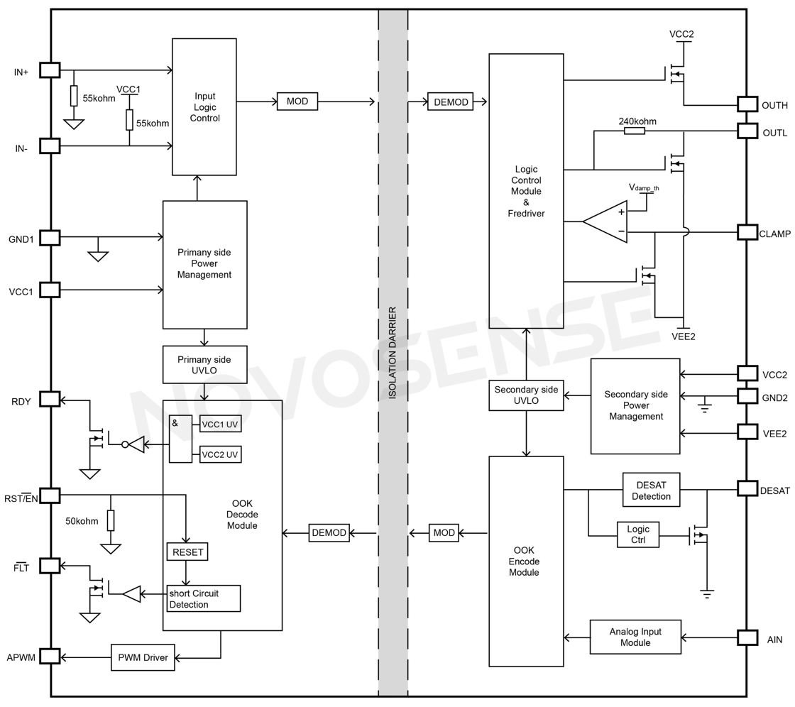
With comprehensive protection functions, including fast overcurrent protection, short-circuit protection, fault soft turn off, 4.5A Miller clamp, and undervoltage protection, this series is a reliable choice for driving power devices such as IGBTs. The entire product family meets the AEC-Q100 standard for automotive applications and can be widely used in new energy vehicles, industrial control and energy management.
Features of NSI67x0 Series
◆ Smart isolation drivers up to 2121Vpk for driving SiC and IGBTs
◆ High CMTI: 150 kV/μs
◆ Input side supply voltage: 3V ~ 5.5V
◆ Driver side supply voltage: up to 33V
◆ Rail-to-rail output
◆ Peak source and sink current: ±10A
◆ Typical propagation delay: 90ns
◆ Operating ambient temperature: -40°C ~ +125°C
◆ Compliant with AEC-Q100 for automotive applications
◆ RoHS compliant package type: SOW16, creepage distance > 8mm

Application Block Diagram of NOVOSENSE NSI67x0 Series
Protection Functions
◆ Fast over-current and short-circuit protection, with optional DESAT threshold voltage of 9V and 6.5V and OC threshold voltage of 0.7V
◆ Integrated soft turn off function in case of fault, with optional soft turn off current of 400mA and 900mA
◆ Integrated Miller clamp function, with clamp current up to 4.5A
◆ Independent undervoltage protection UVLO on both HV and LV sides
◆ Fault alarm (FLT/RDY pin indication)
Isolated Analog Sampling Function
◆ Isolated analog sampling function
◆ AIN input voltage range: 0.3V ~ 4.6V
◆ APWM output duty cycle: 94% ~ 8%
◆ Duty cycle accuracy: 1.6%
◆ APWM output frequency: 10kHz
◆ Optional AIN integrated constant current source output
Safety Related Certification
◆ UL Certification: 1 minute 5700Vrms
◆ VDE Certification: DIN VDE V 0884-11:2017-01
◆ CSA Certification: Approved under CSA Component Acceptance Notice 5A
◆ CQC Certification: Compliant with GB4943.1-2011
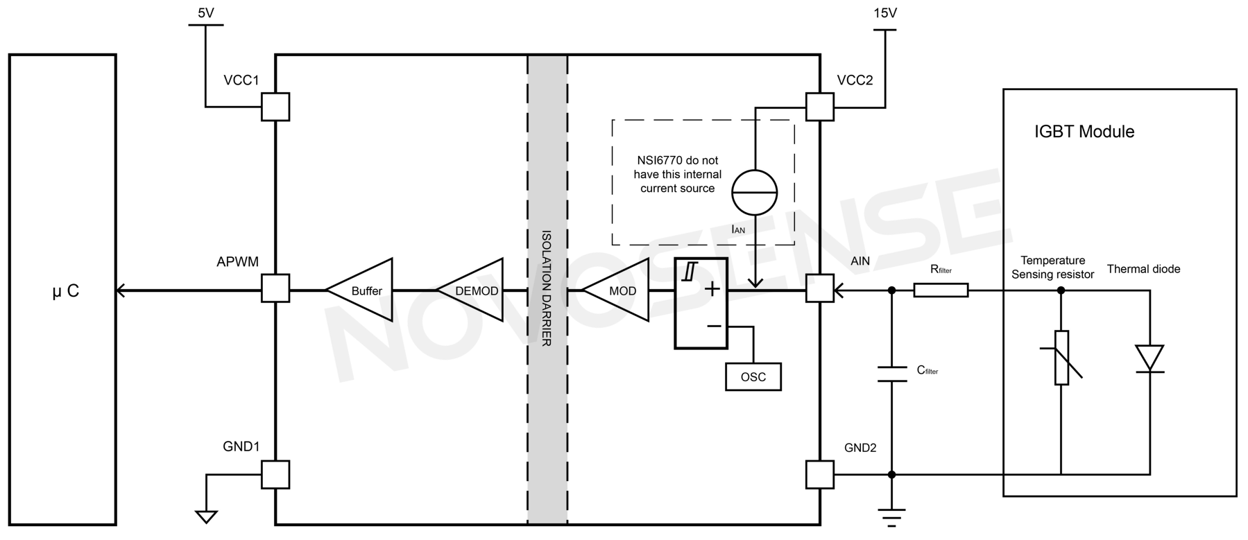
Introduction to Principle of High-precision Temperature Sampling of NSI67x0 Series

Isolated Analog to PWM Sampling Function
The AIN interface of the NSI6730 has a built-in 200uA current source. When an external NTC is connected, a voltage drop will be generated and demodulated into a 10kHz PWM signal for isolated output. The PWM signal is captured by the processor MCU, and the corresponding voltage value and temperature are obtained by calculating the duty cycle.
When the AIN voltage is in the range of 0.2V ~ 4.7V, the AIN input voltage and APWM output duty cycle are linearly related. When the AIN voltage is converted to a PWM signal, the PWM duty cycle conforms to the following formula:
D (%) = 100 - 20 * VIN
That is, the AIN voltage of 0.2V ~ 4.7V corresponds to a PWM duty cycle of 96% ~ 6%.
Model Selection Chart of NSI67x0 Series

This series offers a variety of models to meet the needs of different applications. Specifically, in the NSI67x0 series, when X is 3, the AIN interface integrates a constant current source; when X is 7, the AIN interface does not integrate a constant current source.