
NSI6602-Q1 is a series of highly reliable isolated dual-channel gate driver ICs, which can be designed to drive power transistors with switching frequency up to 2MHz. Each output can source and sink up to 4A/6A with fast propagation delay of 25ns and the maximum delay matching of 5ns. NSI6602-Q1 provides 2500Vrms isolation in a 5*5mmLGA13 package according to UL1577, 3000Vrms isolation in a SOP16 narrow-body package, and 5700Vrms isolation in SOW16 and SOW14 packages. The minimum common mode transient immunity (CMTI) of 100kV/us improves system robustness. The maximum supply voltage of the driver is 28V, and the input side accepts supply voltages from 2.7V to 5V. All supply voltage pins support undervoltage lockout (UVLO). With all these outstanding features, NSI66x2 is suitable for switching power supply systems which require high reliability, high power density and high efficiency.
Product Features
• Isolated dual-channel driver
• Input power supply voltage: 2.7V to 5.5V
• Driver-side power supply voltage: up to 28V with UVLOV
• Peak source and sink current 4A/6A
• High CMTI: ±100KV/μs
• Typical propagation delay: 19ns
• Maximum delay matching: 5ns
• Maximum pulse width distortion: 6ns
• Programmable dead time
• Acceptable minimum input pulse width: 20ns
• operation temperature: -40℃~125℃
• AEC-Q100
• Package form: LGA13 (4*4mm), LGA13 (5*5mm), SOW14, SOW16, SOP16
Safety Certificate
• UL1577 certification:
LGA13: 2.5kVrms for 1 min.
SOW14: 5.7kVrms for 1 min.
SOW16: 5.7kVrms for 1 min.
SOP16: 3kVrms for 1 min.
• CQC certification: Comply with GB4943.1-2011
• CSA certification: Components comply with 5A
• VDE certification: DIN V VDE V 0884-11:2017-1
Application
• Vehicle charger
• Vehicle DCDC
• PTC
• Compressor
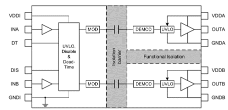
Functional Block Diagram


For more product information, please contact us.