With the popularity of 5G communications and NEVs, there is an increasing demand for high-efficiency power supply. The key factor to improve power conversion efficiency lies in the power part of switching power supply.
Many high-performance, high-frequency PWM control chips, whether of the digital or analog type, have no or limited ability to directly drive a power MOSFET. Since the power MOSFET has high requirements on the gate drive current, the drive chip is equivalent to the bridge between PWM switch control chip and power MOSFET, which is used to amplify the switching signal current and voltage, and has a certain fault isolation ability. Once the selection of a switching power supply scheme is determined, it is necessary to choose the right driver IC, and choose a good driver chip, which requires hardware engineers to have a certain understanding of circuit characteristics.

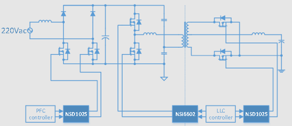
Taking a typical AC/DC switching power supply system as an example, The PFC part adopts the bridgeless PFC topology, an NSD1025 can be used to drive dual low side MOSFETs,. A half-bridge isolated driver chip NSi6602 can be used to drive the upper and lower bridge arm MOSFET at the primary side of LLC, and an NSD1025 can be used to drive the full-wave synchronous rectification MOSFETs at the secondary side. High-speed and high-reliability drive IC can help improve the efficiency and power density of the power supply system.
Since switch power supply often needs hard switch to drive high power load, power MOSFET will often form a large ground bounce voltage and oscillation peak voltage on the input and output of the driver chip in the case of hard switch and layout limitation. The ground bounce voltage can result in an equivalent negative voltage at the driver input. Most gate drivers can withstand a certain amount of negative voltage pulses because of the internal body diode. However, it is necessary to take precautions to prevent excessive overshoot and undervoltage spikes at the driver input from damaging the driver chip or causing misfunction.
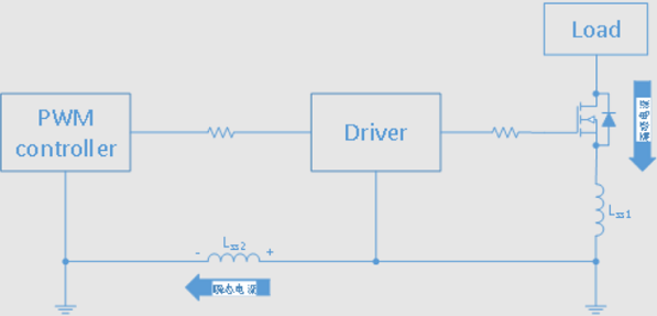
Taking also PFC topology as an example, a low-side driver is used between the control chip and the power MOSFET to help reduce switching losses and to provide enough drive current for the MOSFET to cross the Miller platform area for quick turn-on. When the MOSFET is switched on, a high di/dt pulse is generated. This rapid change and parasitic inductance work together to produce a negative voltage peak, which can be estimated by formula Vn = Lss* di/dt. Lss stands for parasitic inductance. The value of parasitic inductance is approximately equal to the sum of the inductance in the internal bonding line and PCB circuit ground circuit of power MOSFET, and its value can range from several nH to more than ten nH. The size of parasitic inductance mainly depends on PCB layout and wiring.
It can be seen from the above equation that the negative voltage is proportional to the parasitic inductance and current rate of change. In a typical low-side gate drive circuit, the controller and power MOSFET use the same DC ground plane as a reference, but in some cases there will always be parasitic inductance due to the distance between the driver and the controller. When the high di/dt current flows through the MOSFET and its PCB loop, the parasitic inductance will cause the ground potential of the driver to rise instantly relative to the ground potential of the controller, which is equivalent to a temporary negative pressure between the input of the driver and the ground. In extreme cases, the input ESD device inside the driver may be damaged or the driver may fail.

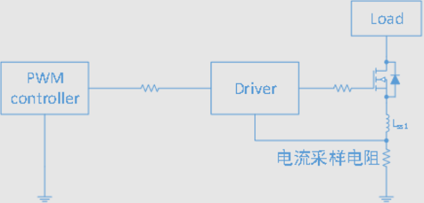
Another common occurrence of negative input voltage is related to current sampling on an MOSFET. For more accurate control, a sampling resistor is sometimes connected between the power MOSFET and the controller ground, which is used to detect the current flowing through the MOSFET, so that the controller can respond quickly. To make the MOSFET drive loop small enough, the GND pin of the driver is connected to the source of the MOSFET, and the GND of the control chip is connected to the real ground plane, so that there is a bias voltage between the GND of the driver and the GND of PWM controller. In this way, when PWM controller output low , there is a negative bias voltage at the input of gate driver relative to its GND pin.

There are generally three solutions to the negative input transients caused by parasitic inductance. First, the impact can be reduced by reducing the switch speed of MOSFETs. Decreasing the switch speed can reduce the current change rate di/dt, and the negative pressure amplitude will drop instantly. But there are side effects. Reducing switch speed increases switching time and therefore switch loss, and in some applications where response time is required, reducing switch speed may not be appropriate.
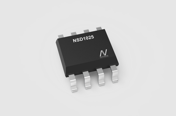
The second method is to optimize PCB layout and wiring as much as possible to reduce parasitic parameters, so as to reduce the peak negative pressure. This is a common approach in system design, but it requires a hardware engineer with very rich design experience, and may not be able to optimize PCB layout and wiring under some design constraints. The third method is to choose a device with strong anti-interference ability, such as the in-phase dual-channel high-speed gate driver NSD1025 launched by NOVOSENSE. By optimizing the ESD structure of the input terminal, NSD1025 can withstand the maximum input voltage of -10V. Compared with other competing products, NSD1025 can better cope with the transient negative pulse in common application scenarios and has better reliability.
Experienced engineers typically consider all three anti-interference schemes at the same time and then make the optimal choice based on the constraints applied. However, the selection of strong anti-interference devices can undoubtedly bring more fault-tolerant space and choice for the design of the whole system, so it becomes the first step for engineers in the system design.
In addition to strong resistance to negative pressure, the NSD1025 also provides undervoltage locking function, which keeps the output level low until the supply voltage enters the operating range, while hysteresis between high and low thresholds also provides superior anti-interference capability. It is ideal for such application scenarios as power supply systems, motor controllers, linear drivers, GaN and other wide-band gap power device drivers.

Besides NSD1025, Novosense also provdie 600V non-isolated half bridge gate driver devices, as well as gate drivers designed for GaN deisgn They can provide engineers with better solutions for anti-interference design in industrial power supplies, motor drivers and other applications.