1) Introduction of the Gate Drivers
Gate driver is a buffer circuit between the low-voltage controller and the high-power circuit, which is used to amplify the control signals of the controller for more effective turn-on and turn-off of power devices.
1. The functions of gate driver are as follows
- Gate driver can convert the low-voltage signal from the controller to higher-voltage drive signal, so as to achieve stable turn-on and turn-off of power devices.
- Gate driver can provide transient source and sink peak currents, which can improve the switching speed of power devices and reduce the switching loss.
- Gate driver can effectively isolate the noise of high-power circuits and protect sensitive circuits against interference.
- Gate driver typically integrates protection functions to effectively prevent damages to power devices.
It can be seen that gate driver is used to ensure better performance of power devices in the system.
2. There are four types of common power devices
- Si-MOSFET devices, which withstand voltage of 20V-650V and are suitable for low-power systems.
- Si-IGBT devices, which withstand voltage of greater than 650V and provide a strong current endurance capability. This type is suitable for high-voltage and high-power systems.
--- Both Si-MOSFET and Si-IGBT are Si-based power devices that have been widely used, and their manufacturing technologies are mature and stable.
- SiC-MOSFET devices, which provide withstand voltage range comparable to IGBT, but feature fast switching speed and low switching loss. They are more suitable for high-voltage and high-power systems.
- GaN devices, currently constrained by the manufacturing technology, typically have a withstand voltage of less than 650V, but provide obviously advantageous switching performance. This power device type is suitable for high-frequency and high-power systems.
--- SiC-MOSFET and GaN devices are wide bandgap semiconductors that boast significant performance advantages over Si-based ones, and will have a broad range of applications in the future.
3. NOVOSENSE gate drivers
Different power devices have varied requirements for gate drivers. Currently, NOVOSENSE has developed driver products suitable for these four types of power devices.

Table 1: Properties of four power device
4. Switching process of power devices
How does a gate driver control the turn-on and turn-off of power devices? Below is a detailed explanation of the switching process of power devices. In power devices, there are equivalent parasitic capacitances, such as CGS, CGD and CDS. The switching process of a power device can be equivalent to the charging and discharging process of its parasitic capacitances.
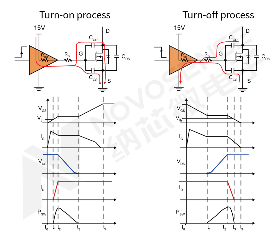
Figure 1: Schematic diagram of the switching process of a power device
4.1 Turn-on process
In the turn-on process, the driver IC connects the output signal to the driver power supply through an internal source current MOS, and charges CGS and discharges CGD through a gate resistor.
- (t0-t1) stage: The gate current charges CGS, and VGS gradually increases. At this point, the power device is still turned off.
- (t1-t2) stage: When VGS increases to a value greater than the gate threshold voltage Vth, the power device begins to turn on, and IDS increases with VGS until it reaches the maximum value.
- (t2-t3) stage: This is the Miller Plateau period, where the gate current mainly discharges CGD, and VDS begins to decrease. The device is fully turned on.
- (t3-t4) stage: The gate current continues to charge CGS, and VGS gradually increases to the power supply voltage. When the gate current reduces to zero, the turn-on process ends. The turn-on loss of the power device mainly occurs at the t1-t3 stage.
4.2 Turn-off process
In the turn-off process, the driver IC connects the output signal to the GND through an internal sink current MOS, and discharges CGS and charges CGD through a gate resistor.
- (t0-t1) stage: The gate current mainly discharges CGS, and VGS gradually decreases.
- (t1-t2) stage: This is the Miller Plateau period, where the gate current mainly charges CGD, and VDS begins to increase. When the voltage reaches VDC, the Miller Plateau ends.
- (t2-t3) stage: IDS begins to decrease. When VGS decreases to Vth, IDS drops to zero, and the power device is completely turned off.
- (t3-t4) stage: The gate current continues to discharge CGS, and VGS eventually drops to zero. The turn-off process ends. The turn-off loss of the power device mainly occurs at the t1-t3 stage.
It can be seen from the analysis above that shortening the t1-t3 stage can effectively reduce the switching loss of power devices.
4.3 Three types of common driver IC
At present, there are three types of commonly used driver ICs, namely non-isolated low-side drivers, non-isolated half-bridge drivers, and isolated drivers.
- Non-isolated low-side drivers are only suitable for power devices with a reference to GND, and provide dual-channel or single-channel driving capability. Non-isolated drivers are relatively simple to implement, requiring only single power supply. They are mainly used in low-voltage systems, such as AC/DC converters, electric tools, and low-voltage DC/DC converters. Currently, NOVOSENSE offers non-isolated low-side driver ICs including NSD1026V and NSD1015.
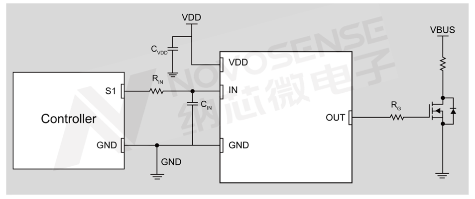
Figure 2: Functional block diagram of non-isolated low-side driver
- Non-isolated half-bridge drivers are used in power systems with a half-bridge configuration. The withstand voltage of the high and low sides is usually achieved through level shifting or isolation, ranging from 200V to 600V. To prevent shoot-through, half-bridge drivers provide an interlock function. When a non-isolated half-bridge driver is used in a system, single power supply plus bootstrap power is typically adopted. This driver IC type is mainly used in low-voltage or high-voltage systems, such as AC/DC converters, motor drives, and on-board DC/DC converters. Currently, the half-bridge driver ICs from NOVOSENSE include NSD1624 and NSD1224.

Figure 3: Functional block diagram of non-isolated half-bridge driver
- Isolated drivers use an internal isolation barrier to physically isolate high and low voltages. Isolated drivers provide flexibility in application. Single-channel and dual-channel isolated drivers are available for low-side, high-side, or half-bridge applications. To achieve primary and secondary isolation in the system, the high-voltage side requires an isolated power supply, making the power supply system relatively complex. Isolated drivers are mainly used in high-voltage systems, such as electric drives, photovoltaic inverters, and OBCs. Currently, NOVOSENSE offers NSI6602 dual-channel isolated driver IC, NSI6601/NSI6601M single-channel isolated driver IC, NSI6801 opto-compatible isolated single-channel driver IC, and NSI6611/NSI68515 smart isolated driver IC.
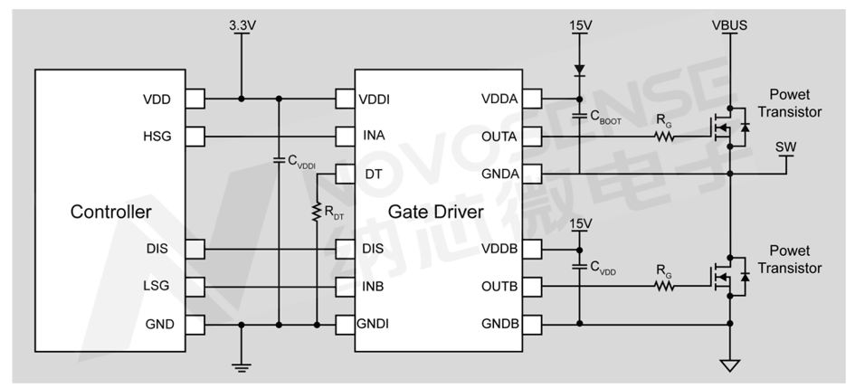
Figure 4: Functional block diagram of isolated driver
2) Introduction to Isolation Solutions
In a high-voltage power system, there is usually isolation between high voltage and high voltage, as well as between high voltage and low voltage. Why is isolation driver needed? First, an isolated driver can avoid harm to human body caused by high-voltage electricity, and meet safety standards through isolation. Second, it can protect the control system from damages that can be caused by lightning strikes and high voltage transients. Third, an isolated driver can eliminate ground loops and reduce interference from the high voltage side to the low voltage side. Fourth, it can realize voltage or current change and energy transfer.
There are three commonly used isolation schemes. The first is optocoupler isolation, which achieves signal transmission through light-emitting diodes and phototransistors. This isolation scheme is low-cost, but provides weak CMTI (Common Mode Transient Immunity), limited temperature range, and short service life. The second isolation scheme is magnetic isolation, where the chip integrates micro-transformer and electronic circuit to achieve signal transmission. The magnetic isolation chips deliver benefits such as long lifetime, wide temperature range, and strong CMTI, but involve complex technology, high cost, and prominent EMI issue. The third isolation scheme is capacitive isolation, which achieves signal transmission through isolation capacitors and electronic circuits. It usually uses silicon dioxide (SiO2) as the insulating material. The capacitive isolation scheme features low cost, long isolation life, wide temperature range, and strong CMTI. NOVOSENSE adopts the capacitive isolation scheme.
NOVOSENSE isolation solution
Isolated driver ICs from NOVOSENSE usually have two dies – the primary die on the input side and the secondary die on the output side. There is a physical isolation between the dies. Two isolation capacitors are connected in series on the die to achieve double insulation capability. If one of the dies experiences an EOS failure, the driver IC can still maintain basic insulation capability. The top and bottom substrates of the two isolation capacitors are insulated using SiO2, which can ensure stable material properties, good chip consistency, and long isolation life. The top substrates of the two isolation capacitors are connected by metal wires for signal transmission. NOVOSENSE’s isolated driver ICs can withstand surge voltage up to 12kV and 8kV transient insulation voltage test, far exceeding the insulation requirements of high-voltage systems.
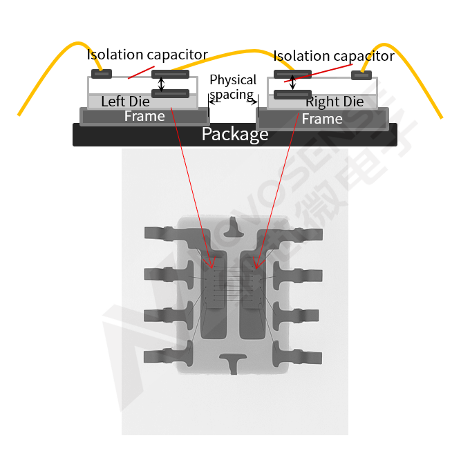
Figure 5: Position reserved and text to be determined
The communication between the dies adopts the differential OOK modulation scheme, which ensures stable and reliable communication. The input signal is modulated at a high frequency and then transmitted from the primary die to the high-voltage die through the isolation capacitor, with the modulation frequency at a level of over 100 MHz. A proprietary CMTI modular circuit is added at the input side of the differential signal, allowing the IC to achieve a stronger CMTI capability up to 150V/ns. For power systems with a high dv/dt, the IC can still work stably without abnormal wave emission.
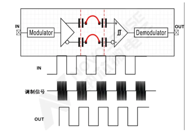
Figure 6: Position reserved and text to be determined