Because of the working principle of LDO, it can not only provide high power quality at low cost, but also inevitably bring loss and heating problems. In the case of large voltage drop and large current, LDO will be in a higher working temperature range for a long time, which may affect its working life and reliability. Therefore, by analyzing and evaluating the temperature of LDO under specific working environment in advance, and then taking certain measures, we can effectively avoid chip thermal shutdown and aging under long-term high temperature.
The junction temperature of a chip is mainly determined by its power consumption, heat dissipation conditions and ambient temperature. Therefore, selecting different packaging versions to reduce the thermal resistance of the chip junction to the environment has become one of the effective solutions to reduce the junction temperature.
Contents
1. Thermal Resistance in The Chip
2. Thermal Analysis Using Thermal Resistance Matrix
2.1. Misunderstanding of θJA.
2.2. Understanding of ΨJC &θJC
3. LDO Junction Temperature & Thermal Resistance Test on EVM
1. Thermal Resistance in The Chip
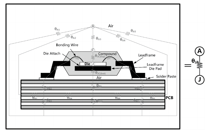
In the engineering practice of chip application, due to the complex structure of the chip, the theoretical calculation of thermal resistance is usually completed by simulation. Usually, engineers combine theoretical thermal resistances into categories with practical application problems, resulting in some thermal resistances that have obvious physical meanings. The figure below shows the thermal resistance network when the chip is welded on the PCB.

Figure 1 Thermal Resistance Network of Chip
In the figure, the heat is transferred from the junction up through the package body to the top of the package case, and the sum of the thermal resistances between them is denoted as θJC(top). In addition, the heat is transferred from the junction down through the adhesive, the leadframe die pad, to the bottom thermal pad and the entire PCB, with the sum of the thermal resistances denoted by θJB. Also, the unified thermal resistance of all the heat from the junction to the external environment in all directions for all materials and structures is denoted as θJA.
Although these thermal resistances can be obtained through the deterministic simulations, they may be inaccurate due to manufacturing errors and other reasons. Therefore, the thermal resistance is often measured by the chip heat generation and temperature difference in engineering. Here is the definition of thermal resistance:

This means that whether it is to reduce the heat generation of the chip, switch to a larger package with better heat dissipation, increase the heat sink and fan, improve the PCB heat dissipation design, etc., the temperature rise of the chip can be reduced.
2. Thermal Analysis Using Thermal Resistance Matrix
2.1 Misunderstanding of θJA
Usually we can find a thermal resistance information matrix in the datasheet of the chip, which contains the parameters such as θJA and θJC(top) mentioned above. The following table is taken from the datasheet of the NSR31 series LDO.

Table 1 Thermal Information of NSR31 Series
It is worth noting that chip application personnel often use θJA, ambient temperature and chip power dissipation to calculate junction temperature, which may lead to large calculation errors.
As can be seen from the definition of θJA in Figure 1 of the previous section, its value is not only determined by the chip itself, but also largely depends on the application PCB. The heat dissipation area, number of layers, copper thickness, board thickness, material, and device layout of different application PCBs are different, so each different PCB has a very different θJA value. Most chip application personnel are mainly concerned with what happens on their own application PCB. Therefore, it is not recommended to use θJA in thermal design. The benefit of using θJA is to compare the thermal performance of different package types.
θJA on almost all chip datasheets is usually an example value measured or simulated using industry standard boards. These industry standard platforms are called JEDEC High-K or JEDEC Low-K boards. Furthermore, these JEDEC boards (consisting of only one IC device mounted on a large 3" x 3" area) are significantly different from the actual PCB.
2.2 Understanding of ΨJC & θJC
To solve the practical problems on the application side, the thermal characterization parameter Ψ is also given in the table. This is a thermal metric defined by the Joint Electron Device Engineering Council (JEDEC) in the 1990s. It is a more convenient indicator for estimating the junction temperature of modern package type devices. It simply represents the ratio of the temperature difference between the junction and the reference point to the total power dissipated by the chip. It's just a coefficient, and while the formula and units (°C/W) are very similar to Rθ, Ψ is not really a thermal resistance parameter, it's defined as:

Among them, ΨJC is the thermal characterization parameter from junction to case, TJC is the temperature difference from junction to case, and PD is the total dissipation power of the chip. Therefore, when we want to ask for TJ, first measure the case temperature TC, calculate the total dissipation power PD of the chip, and use the following formula:

Among them, ΨJC can be obtained from obtained from the thermal resistance information matrix in datasheet. When the external heat dissipation conditions of the chip are fixed, YJC is proportional to θJC. Compared with the vastly different θJA of the application side, although ΨJC is also affected by the heat dissipation capability of the PCB, it can be approximated that the influence is not significant in most applications. The specific reasons are as follows.
Equation (2-2) can be further written as:

where PC is the thermal power transferred from the junction up through the package to the top of package case. Then we can get:

That is, ΨJC is proportional to θJA, and the value is the ratio of the thermal power from the junction to the top of the case to the total dissipation power of the chip.

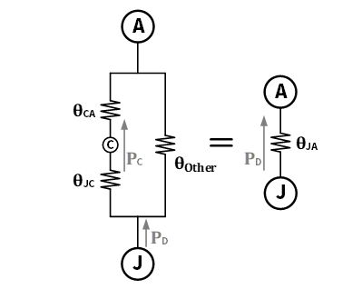
Figure 2 Simplified Chip Thermal Resistance Network
Further, as shown in Figure 2, according to the "Current Division Formulas of the Parallel Resistance" relationship of the thermal resistance linear network, the power ratio is equivalent to the inverse of the thermal resistance ratio:

In the formula, θCA is the thermal resistance from the case to the environment. When the surface heat sink is not installed, θCA is much larger than θJC. It can be seen that ΨJC is less than θJA, so the error of ΨJC in actual PCB will be much smaller than the error of θJA during application. Further, the evaluation calculation of the junction temperature can be made more accurate.
3. LDO Junction Temperature & Thermal Resistance Test on EVM
The junction is not exposed because the mold compound is wrapped outside the integrated circuit, so we cannot directly measure the temperature of the junction inside the chip through a thermocouple or an infrared thermometer. For many large packaged integrated circuits, such as CPUs or GPUs, there is usually an integrated thermal sensor for TJ measurement. However, for small packaged integrated circuits, this TJ sensor function is not available due to the limitation of the size of the silicon. Therefore, we must estimate TJ through testing and thermal analysis.
For NSR31/33/35 series LDOs, there are 8 packages, the specific information is shown in the table 2. Various types of thermal resistances of different packages have been indicated in the thermal resistance matrix of the chip datasheet. The information is summarized as follows.

(1) The thermal data is based on the JEDEC standard high-K profile, JESD 51-7, four layer board.
In Table 2, all parameters are obtained under JEDEC standard. Compare from the table θJA can know that SOT-23-5L package has the worst thermal performance, while TO263-5 package has the best thermal performance. For LDOs, when we want to obtain the junction temperature on our own application circuit board, we can use Formula (2-2) :

Where, VIN represents LDOs input voltage, VOUT represents LDOs output voltage, and IOUT represents LDOs output current.
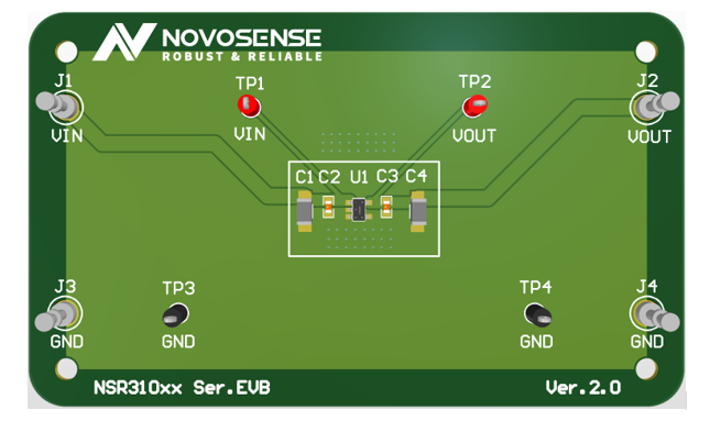
The following example will be NSR31050-QSTAR, the junction temperature and actual thermal resistance θ'JA were measured and calculated on EVM board for reference. Specifically, the EVM board uses a four-layer design (88mm x 53mm), with a copper thickness of 1 ounce and a total heat dissipation area of about 4600 square millimeters, as shown in Figure 3.

Figure 3 NSR31050-QSTAR EVM Board
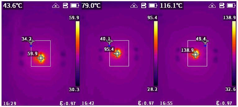
Under the condition of constant room temperature ventilation, by applying a certain voltage and load to the LDO, the power consumption can be increased from 0W to nearly thermal shutdown. At various power consumption settings, keep the temperature stable for 5 minutes and use the handheld infrared thermometer to measure the top case temperature of the chip. The junction temperature and the thermal resistance θ'JA of the chip on the EVM board were estimated and averaged by a formula combining with the ambient temperature, case temperature, power consumption and ΨJC. The results are shown in table 3.

Table 3 Thermal Information of NSR3x Series

Figure 4 Results of Partial Case Temperature Infrared Measurement
As can be seen from Table 3, on this EVM board, the measured thermal resistance θ'JA from junction to environment is about 77.5°C/W, which is much smaller than 207.9°C/W under JEDEC standard.
In summary, in practice, there are a variety of heat conduction pathways, and heat is transported through multiple channels. It is difficult to estimate the power consumption of a particular path in the same way as the total power consumption. For these reasons, the thermal characteristic parameter ΨJC is more suitable to estimate the junction temperature. Therefore, it is necessary to use the thermal characteristic parameter ΨJC combined with formula (3-1) to estimate the junction temperature.