2024/02/20
The main drive electronic control system is an important part of a new energy vehicle. This article will start from the system block diagram of the electronic control system, introduce the components of the system and their functions, and focus on the use of NOVOSENSE's single-channel isolated driver with protection function NSI6611, in the electronic control system: its Miller clamp function can well prevent short circuits; and the DESAT function can shut down IGBT / SiC in time when a short circuit occurs, protecting IGBT / SiC from damage and ensuring safe and stable operation of the system.
Contents
1)Introduction to the main drive electronic control system driver and the NSI6611-based driver board
1. Composition of the main drive electronic control system
2. Main chips on the driver board
3. Interface definition
4. NSI6611 application circuit
2)Introduction to Miller clamp and the active Miller clamp function of NSI6611
1. Miller effect
2. Active Miller clamp
3. Short circuit detection of power devices
3)Introduction to the DESAT protection function of NSI6611
1. DESAT detection peripheral circuit configuration and parameters
2. DESAT protection timing
3. Soft turn-off function
1) Introduction to the main drive electronic control system driver and the NSI6611-based driver board
1.1 Composition of the main drive electronic control system
The main drive electric control system consists of low voltage battery, VCU, MCU, high voltage battery and resolver three-phase motor. As shown in Figure 1 below, inside the blue dotted line is the main drive motor controller part and inside the red dotted line is the driver board that will be highlighted in this article.
Functionally, the low voltage battery provides low voltage power supply for the system, and the VCU sends instructions to the electronic control system via the CAN bus and reads the status of the electronic control system; the high voltage battery provides high voltage power supply, and the Flyback circuit provides positive and negative voltages for the IGBT driver to drive the three-phase motor; the LDO (low dropout linear regulator) provides +5V power supply for the driver chip. NOVOSENSE's high voltage isolated driver NSI6611 is used to drive the IGBT and SiC modules; the current sampling circuit and resolver-to-digital converter are used to control motor operation.
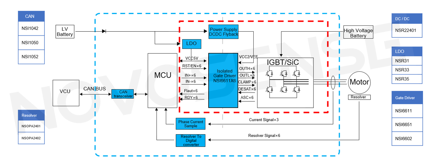
Figure 1: Block diagram of the main drive electronic control system
In the main drive electronic control system, NOVOSENSE provides a variety of chips, including the CAN interface chip, resolver-to-digital converter, power supply chip and high voltage isolated driver chip.
1.2 Main chips on the driver board
Figure 2 below is a three-phase drive circuit board designed based on NOVOSENSE's single-channel smart isolated driver NSI6611. The six chips in the blue boxes are all NSI6611. The driver board also uses NOVOSENSE's Flyback power control chip NSR22401 to provide positive and negative voltages for the high voltage drive side of NSI6611; the LDO chip NSR3x provides 5V power supply for the low voltage side of NSI6611.
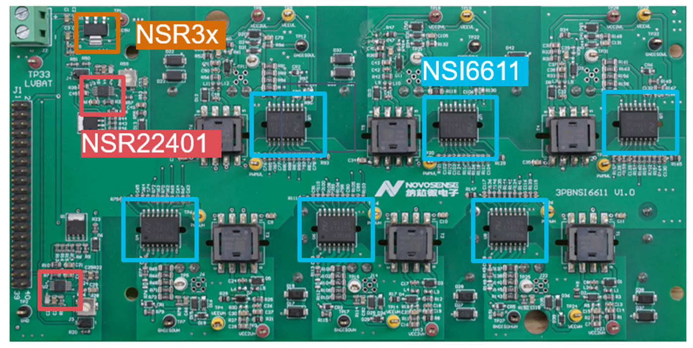
Figure 2: Driver board based on NOVOSENSE NSI6611
NSI6611 is an automotive-grade, high voltage isolated gate driver with protection function that can drive IGBTs and SiCs, and it supports a peak voltage of up to 2121V and a maximum drive current of 10A without the need for an external drive circuit; CMTI (common-mode transient immunity) can be as high as 150kV/μs. In addition, it integrates active Miller clamp and DESAT (desaturation) protection, soft turn-off and ASC (active short circuit) functions internally, with an operating temperature range of -40°C to +125°C.
1.3 Interface definition
As shown in Figure 3 below, the left side of the driver board is the signal interface between the driver board and the control board, including 6 input signals provided by the control board for PWM control; 6 FAULT output signals provided to the control board when NSI6611 detects IGBT overcurrent or undervoltage; 6 Ready output signals used to indicate whether the NSI6611 power supply is undervoltage; and 2 RESET input signals that control 3 high sides and 3 low sides respectively. The right side of the driver board is the power interface, and the power supply voltage range is 9V to 16V.
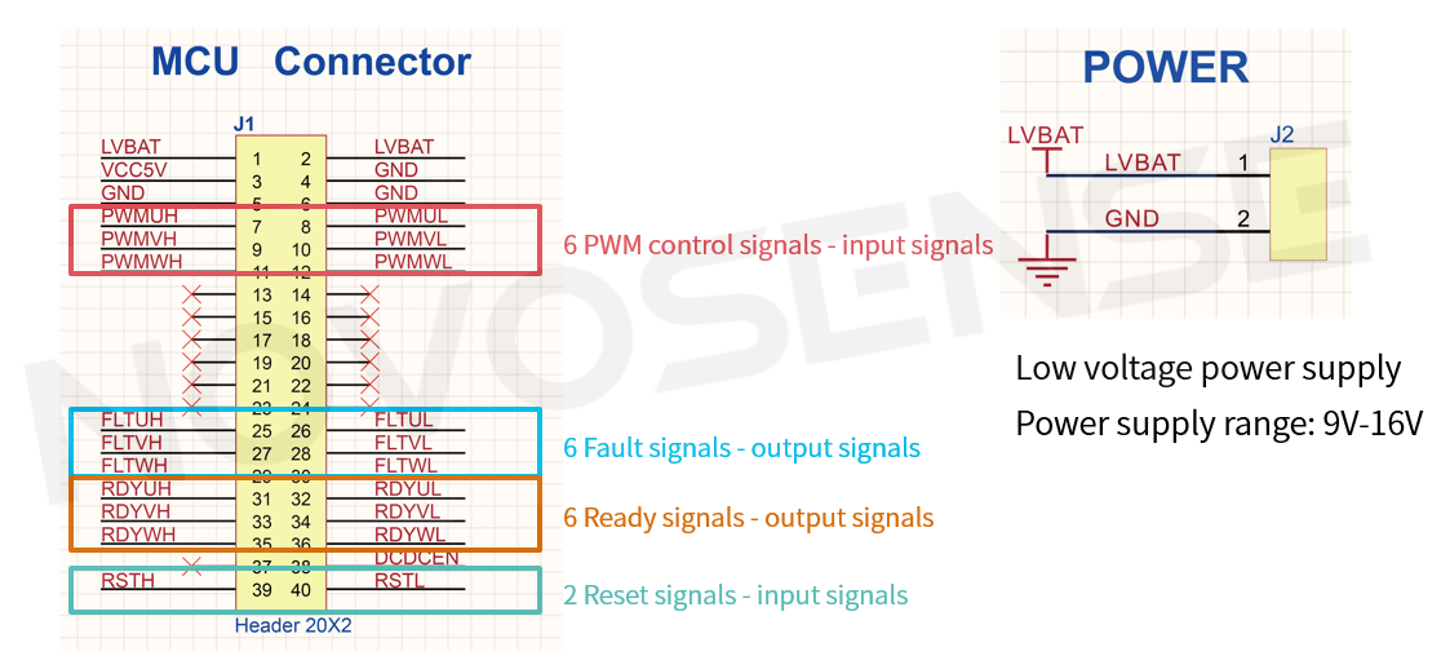
Figure 3: Interface definition of the driver board
1.4 NSI6611 Application Circuit
Figure 4 below is the drive circuit of NSI6611. The left side is the low voltage control side. The 100Ω resistor connected in series on the signal line can effectively reduce signal reflection; since the Fault and Ready signals have an internal Open Drain structure, a 5.1kΩ pull-up resistor needs to be added. In addition, the RC circuit composed of the PWM signal and a 1nF capacitor can filter out high-frequency signals, and a 0.1μF decoupling capacitor is added to VCC1.
The right side is the high voltage drive side. Two 1206 package gate resistors are connected in parallel. The gate has a 10k pull-down resistor. The gate capacitance can be adjusted for different applications. The CLAMP pin is connected to the GATE through a 0Ω resistor.
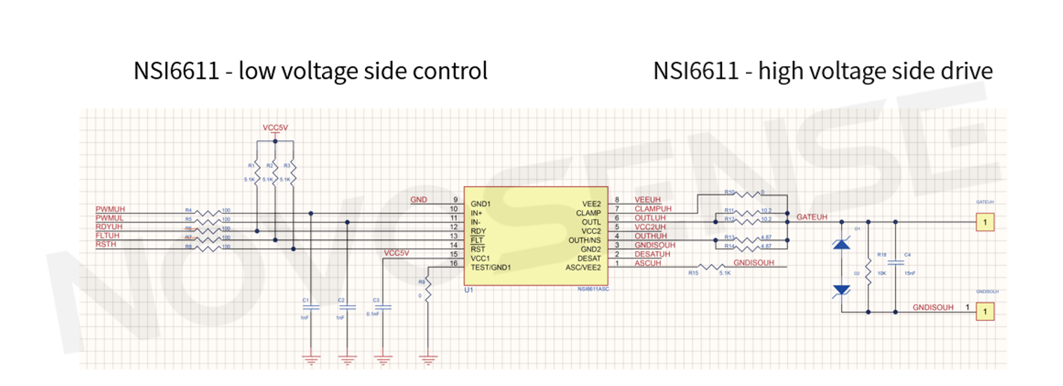
Figure 4: Drive circuit of NSI6611
2) Introduction to Miller clamp and the active Miller clamp function of NSI6611
2.1 Miller effect
The Miller effect refers to the phenomenon in a transistor or field effect tube that the capacitance at the output of the amplifier increases due to the interaction between the input capacitance and the gain of the amplifier. It can not only increase switching delay, but also cause parasitic turn-on.
Due to the inherent characteristics of semiconductors, there are various parasitic capacitances inside the IGBT. The capacitance between the gate and collector is called Miller capacitance. It is often seen in tests that the gate voltage does not rise directly to the VCC voltage, but rises to a voltage plateau, maintains for a period of time and then rises again. This voltage plateau is the Miller plateau, which is generated by Miller capacitance.
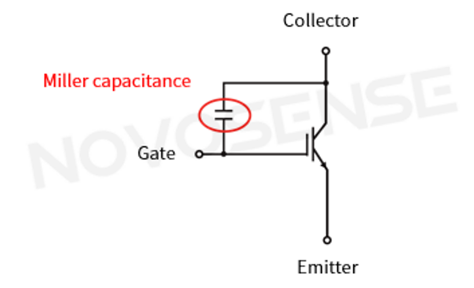
Figure 5.1: Miller effect
Miller capacitance may also cause false turn-on of the low side. Typically, motor drives require the use of the high and low sides. When Q2 is turned off and Q1 is turned on, a certain current will be generated due to the high dv/dt and Miller capacitance. We can calculate the current by using the formula I=C * dv/dt. The current flowing through the gate resistor will generate a VGE voltage. When this voltage exceeds the turn-on threshold of Q2, Q2 will turn on, and at this time, Q1 is already in the ON state, thus causing a shoot-through short circuit.
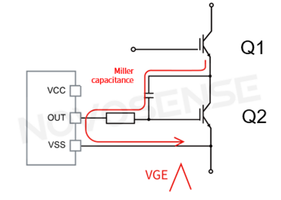
Figure 5.2: Miller effect
2.2 Active Miller clamp
In order to solve the problem of shoot-through caused by the Miller effect, negative voltage turn-off can be used, but this will increase the complexity of the power supply design and increase the BOM cost; the second option is to use a driver chip with Miller clamp function to control the IGBT turn-off process.
The IGBT turn-off process controlled by a driver chip with Miller clamp function is shown in Figure 6 below. First, the OUTL pin is turned on, causing the gate voltage to drop; when the gate voltage drops below the CLAMP threshold, the CALMP pin is turned on, causing the OULT pin to turn off. The resulting path can effectively bypass the gate resistor, thus avoiding the phenomenon of shoot-through. It is worth noting that the Miller clamp module only works when the IGBT is turned off.
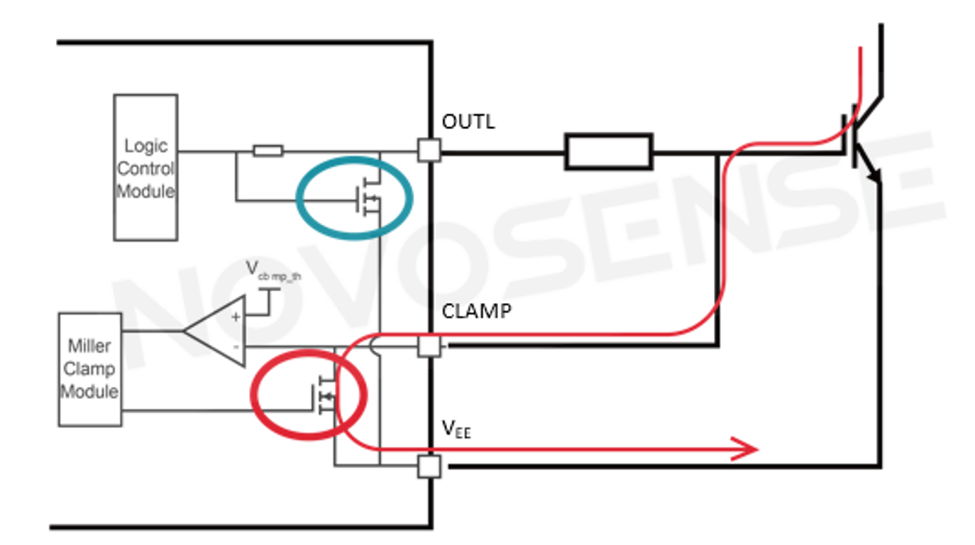
Figure 6: Schematic diagram of the IGBT turn-off process controlled by a driver chip with Miller clamp function
2.3 Short circuit detection of power devices
IGBT and SiC devices vary in their short circuit capabilities. Before using a power device to design a drive system, you must first understand its basic parameters such as maximum voltage, maximum current and Rdson (on-resistance). Short-circuit capability is also a parameter worthy of focus, since the short circuit characteristics of the device need to be known when short circuit protection is designed.
Take the short circuit characteristic parameters of the IGBT as an example. At 25°C, its maximum short circuit time is 6μs, which means that the IGBT needs to be turned off in time within 6μs. When the short circuit current reaches 4800A, the value is already several times the normal operating current. Once a short circuit occurs, a large amount of heat will be generated instantly, causing the junction temperature to rise sharply. If it is not turned off in time, the device will be burned and there is even a risk of fire. This must be avoided in system design.
Generally, the short circuit time of IGBT can reach up to 10μs, while the short circuit time of SiC is only 2~3μs, which brings great challenges to short circuit protection. Therefore, short circuit must be detected and turn-off must be performed in time.
Method 1 is current detection. A resistor is connected in series with the IGBT, or a current sensor is used to directly detect the overcurrent condition. However, this will increase the cost significantly and make the circuit system more complex.
Method 2 is desaturation detection, also known as DESAT protection. As shown in Figure 7 below, we can see from the graph of VCE voltage and collector current that when VCE is less than 0.4V, no current flows through the cut-off region; as the VCE voltage increases, the current also increases and a saturation region appears, and then it enters the linear region, i.e., the desaturation region.
Usually, when the IGBT works in the saturation region, it will enter the desaturation region once a short circuit occurs. It can be seen that the VCE voltage generally does not exceed 2V in the saturation region; if it enters the desaturation region, VCE will rise rapidly and even reach the system voltage. Desaturation detection is to detect whether the IGBT has entered the desaturation region by detecting the VCE voltage.
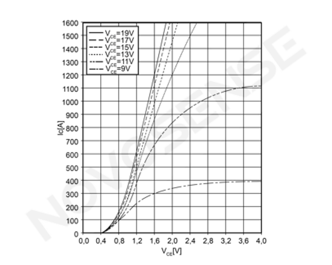
Figure 7: Schematic diagram of short circuit detection for power devices
3) Introduction to the DESAT protection function of NSI6611
3.1 DESAT detection peripheral circuit configuration and parameters
DESAT detection consists of NSI6611 and external DESAT capacitor, resistor and high voltage diode. The NSI6611 chip integrates a 500μA constant current source and comparator internally.
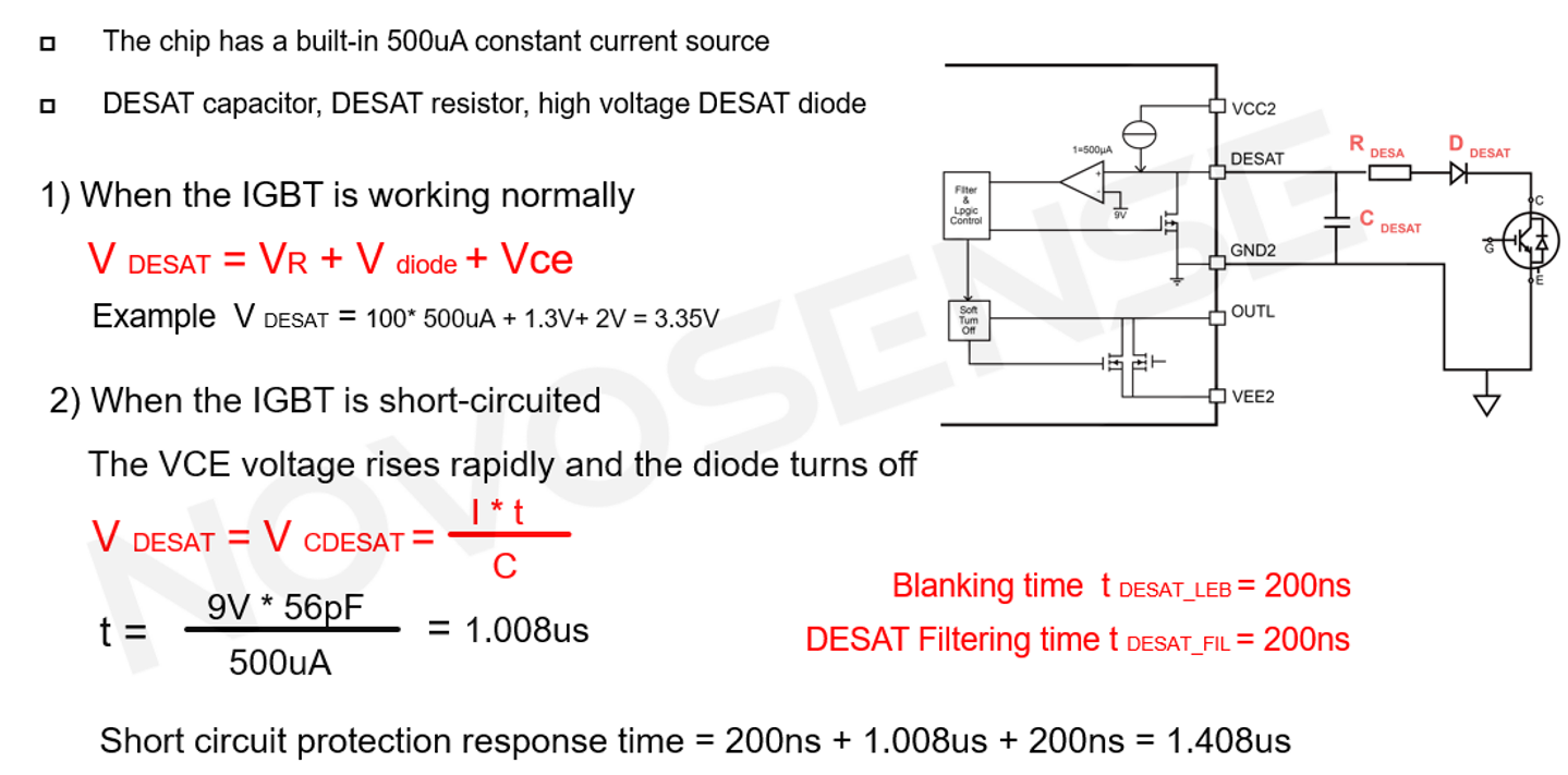
Figure 8: DESAT detection peripheral circuit configuration and parameters
When the IGBT is turned on normally, the VCE voltage is very low, basically below 2V, and the diode is in a forward turn-on state. The voltage value of VDESAT is equal to the voltage drop of the resistor plus the voltage drop of the diode, plus the VCE voltage. Assuming that the resistance of the resistor is 100Ω, the forward voltage drop of the diode is 1.3V, and VCE is 2V, then, according to the formula in Figure 8, we can get: When the IGBT is turned on normally, the voltage detected by DESAT is basically less than 3.35V.
When the IGBT is short-circuited, the VCE voltage will rise rapidly. At this time, the diode is in the OFF state, and the current will flow to the DESAT capacitor and charge it. Since the DESAT current of NSI6611 is 500μA and the DESAT threshold is 9V, this means that a capacitor needs to be matched to charge the DESAT capacitor to 9V at 500μA within the short circuit time.
Assuming that the DESAT capacitance is 56pF, according to the capacitor charging formula in Figure 8: the charging time of the capacitor is about 1μs; plus the blanking time of 200ns and the filtering time of 200ns, the total short circuit protection response time is 1.4μs. This time is not only shorter than the safe short circuit time of IGBT, but also shorter than the safe short circuit time of SiC.
3.2 DESAT protection timing
Figure 9 below is the DESAT protection timing diagram. It can be seen from the figure that in step 1, GATE rises and DESAT starts the blanking time; in step 2, the blanking time ends and the DESAT current is turned on, and if the IGBT is short-circuited, the diode enters the cut-off state and the DESAT current charges the capacitor; in step 3, when the DESAT capacitor is charged to the threshold of 9V, the filtering time of DESAT protection starts; in step 4, the filtering time ends and GATE is turned off.
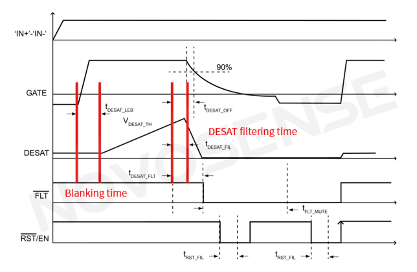
Figure 9: DESAT protection timing diagram
3.3 Soft turn-off function
As mentioned above, GATE is turned off when a DESAT fault is detected. So, is it enough to just turn it off normally? Not really. When a short circuit occurs, the IGBT current is at least 6 to 8 times the normal current. According to the formula, the voltage is equal to the stray inductance of the system multiplied by di/dt (V=Ls*di/dt). If such a large current is turned off quickly, a large VCE voltage will inevitably be generated, which is enough to damage the IGBT. There are only two ways to reduce VCE overshoot: one is to reduce stray inductance, and the other is to reduce di/dt.
Firstly, due to the parasitic parameters of the device, PCB routing, structural design, etc., there is inevitably a certain amount of stray inductance; secondly, to reduce di/dt, under the premise of a certain current, the only way is to increase the turn-off time, that is, let the IGBT turn off slowly for safe turn-off. NSI6611 can provide 400mA soft turn-off, thereby suppressing VCE overshoot and effectively solving the problem of device protection.
NOVOSENSE's single-channel gate driver with protection function, NSI6611, has passed AEC-Q100 reliability certification and has been installed in batches at many carmakers. To request samples, you can email sales@novosns.com or call 0086-512-62601802 for consultation.